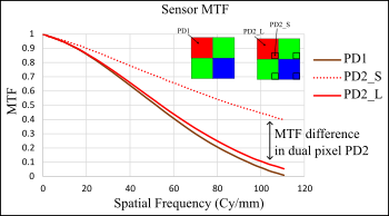
High dynamic range (HDR) image sensors have become increasingly important for automobile applications, particularly for advanced driver-assistance systems (ADAS) in recent years. The traditional single photodiode and split photodiode pixels are the two most commonly used technologies to build HDR image sensors in the industry. This study used a monochrome CMOS image sensor to model single and split photodiode pixel images to examine image quality. Slanted edge images were used to calculate the spatial frequency response (SFR), and the results showed a significant difference in modulation transfer function (MTF) from the split photodiode. MTF of the large photodiode in the split photodiode pixel at half Nyquist was lower than MTF of the small photodiode, as expected. However, the sampling area and the spatial separation of the small photodiode in the split pixel caused edge artifacts in the image. The traditional single photodiode pixel does not experience a change in MTF with light level and edge artifacts were not observed.

Can a mobile camera see better through display? Under Display Camera (UDC) is the most awaited feature in mobile market in 2020 enabling more preferable user experience, however, there are technological obstacles to obtain acceptable UDC image quality. Mobile OLED panels are struggling to reach beyond 20% of light transmittance, leading to challenging capture conditions. To improve light sensitivity, some solutions use binned output losing spatial resolution. Optical diffraction of light in a panel induces contrast degradation and various visual artifacts including image ghosts, yellowish tint etc. Standard approach to address image quality issues is to improve blocks in the imaging pipeline including Image Signal Processor (ISP) and deblur block. In this work, we propose a novel approach to improve UDC image quality - we replace all blocks in UDC pipeline with all-in-one network – UDC d^Net. Proposed solution can deblur and reconstruct full resolution image directly from non-Bayer raw image, e.g. Quad Bayer, without requiring remosaic algorithm that rearranges non-Bayer to Bayer. Proposed network has a very large receptive field and can easily deal with large-scale visual artifacts including color moiré and ghosts. Experiments show significant improvement in image quality vs conventional pipeline – over 4dB in PSNR on popular benchmark - Kodak dataset.

In this paper we propose a low power consumption high speed analog correlated multiple sampling (CMS) technique with high density switched capacitors for low noise CMOS image sensors. A CIS with 256 analog memories per pixel using high density trench capacitors was employed in order to verify the noise reduction effect dependent on operation timings. The noise characteristics were measured at sampling numbers of M=1~64 with various CMS sampling period of 10ns to 1µs and time interval between reset and signal samplings, thanks to the high flexibility owing to the proposed analog CMS technique. The measurement results agree well with the theoretical calculation results, showing that conducting CMS with highly correlated signals is effective in noise reduction.

This paper presents an effective tuning framework between CMOS Image Sensor (CIS) and Image Signal Processor (ISP) based on user preference feedback. One of key issue in ISP tuning is how to apply individual's subjectivity of Image Quality (IQ) in systematic way. In order to mitigate this issue, we propose a framework that efficiently surveys user preference of IQ and select ISP parameter based on those preferences. The overall processes are done on large-scale image database generated by an ISP simulator. In preference survey part, we make clusters that consist of perceptually similar images and gather user’s feedback on representative images of each cluster. Next, for training user preference, we train a DNN model according to general preference, and fine-tune model to optimize individuals preference based on user feedback. The model provides ISP candidate most similar to the preferences. In order to assess performance, the proposed framework was evaluated with a state-of-art CIS and ISP system. The experimental results indicate that the proposed framework converges the IQ score according to user feedback and find the ISP parameters that have higher quality IQ as compared with hand-tuned results.

An indirect time-of-flight (ToF) CMOS image sensor has been designed with 4-tap 7 μm global shutter pixel in back-side illumination process. 15000 e- of high full-well capacity (FWC) per a tap of 3.5 μm pitch and 3.6 e- of read-noise has been realized by employing true correlated double sampling (CDS) structure with storage gates (SGs). Noble characteristics such as 86 % of demodulation contrast (DC) at 100MHz operation, 37 % of higher quantum efficiency (QE) and lower parasitic light sensitivity (PLS) at 940 nm have been achieved. As a result, the proposed ToF sensor shows depth noise less than 0.3 % with 940 nm illuminator in even long distance.

This study investigated the noise suppression effect of multiple sampling applied to a 3-stage pipeline analog-to-digital converter (ADC) in a 33-megapixel, 120-fps 1.25-in CMOS image sensor. The 3-stage pipeline ADC is composed of folding-integration (FI), cyclic, and successive approximation register ADCs, and the multiple sampling for noise suppression is implemented in the FI ADC. The sampling number M is limited by the conversion interval of the FI ADC and the maximum sampling number is M=6 at the 120-fps operation. To investigate the noise suppression effect of 120-fps operation, we measured the random noise of the pixel readout circuit to the sampling number M and compared with theoretical calculations. As a result, we confirmed that the measurement result corresponds reasonably well with the calculated result and the sampling number M = 6 is effective for noise suppression. Furthermore, the calculations revealed that the influence of 1/f noise of the source follower is dominant on the noise performance.

For several decades, many CMOS Image Sensors (CIS) with a small pixel size have used single slope column parallel ADCs (SS-ADC). It is well known that the main drawback of this ADC is the conversion speed. This paper presents several ADC architectures which improve the speed of a SS-ADC. Different architectures are compared in terms of ADC resolution, power consumption, noise and conversion time.